Saturday, July 24, 2010

OpenSPARC T1 and T2 Processor Implementation

CMT

As discussed previously, OpenSPARC gives preference to parallel computation rather than long pipelined instructions. Here is a diagram to summarize the concept


Most of the time, the processor will be stalled waiting on the memory or I/O operations.


OpenSPARC T1 OVERVIEW AND COMPONENTS

OVERVIEW:

OpenSPARC T1 consists of eight physical cores, each core having hardware support for 4 threads (strands or virtual processor). The four strands run simultaneously, with the instructions from the four strands being executed in a round robin fashion. If a single strand gets stuck with a long latency event, then the round robin continues for the remaining 3 strands till the 4th strand becomes available again.


It has a 64 entry, fully associative TLB which is shared by the 4 strands. The 8 cores are connected to the 12-way associative L2 cache through CCX (Cache Crossbar Switch). You can see in the diagram that 4 lines are entering the J-Bus and 8 are connected to the 4 DRAM control channels which are connected to DDR2-SDRAM.


COMPONENTS

  • OpenSPARC T1 Physical Core

Each core has support for 4 threads. They have a register file per strand. Each register file has 8 register windows. Most of the ASI (Address Space Identifier), ASR (Ancillary State Register) and privileged registers are replicated per strand.


The 4 strands share the instruction and data caches and TLBs. Multiple strands can update the TLB without locking using the "Autodemap" feature.

Six stages in core-pipeline

1. Fetch
2. Switch
3. Decode
4. Execute
5. Memory
6. Writeback


Switch stage consists of strand instruction register for each strand. Strand scheduler picks up a strand and the current instruction for that strand is passed into the pipe. Simultaneously, the hardware fetches the next instruction for that strand.

It is then decoded in the Decode stage. The register file access occurs at the same time.

In the Execution stage, all arithmetic and logical operations take place. Memory address is also calculated at this stage. The data cache is accessed in the memory stage and the instruction is committed in the Writeback stage. All traps are signaled in this stage.

As was mentioned in the previous post, round robin scheduler is used by the scheduler to assign instruction to a strand. If a long latency instruction is received by a strand, it is not scheduled till the time it is not completed.


  • FPU
A single FPU is shared amongst all eight cores.

  • L2 cache
Its banked 4 ways

  • DRAM Controller
Each L2 cache bank interacts with exactly one DRAM controller. The CMP frequency must be 4xDRAM controller frequency.

  • I/O Bridge Unit
The IOB performs an address decode on I/O addressable transactions and directs them to the appropriate internal block or to the appropriate external interface.

  • J-Bus is the interconnect between the T1 and the I/O subsystem.
  • Clock and Test Unit
CTU contains the clock generation, reset and JTAG circuitry.

T1 has a single PLL which takes the J-Bus clock as its reference, where the PLL output is divided down to generate the CMP clock.


Summary of Differences between T1 and T2:

I MICRO-ARCHITECTURAL DIFFERENCES

OpenSPARC T2 has two integer execution pipelines whereas T1 has one.

Each physical core in T2 has 8 strands which are divided into 4 strands each sharing a single integer pipeline. Whereas T1 core has 4 strands sharing a single integer pipeline.

Sunday, May 30, 2010

Architecture Overview

The OpenSPARC T1 design is based on theUltraSPARC Architecture 2005, and OpenSPARC T2 is based on the UltraSPARC Architecture 2007.


THE ULTRA SPARC ARCHITECTURE


Here I will be listing out a few of the important architectural features of UltraSPARC.

Hardware Trap Stack: A hardware trap stack is provided to allow nested traps. It contains all of the machine state necessary to return to the previous trap level.

Hyperprivileged Mode: This mode simplifies porting of operating systems and provides robust handing of error conditions.

Extended Instruction Set: It includes many instruction set extensions.

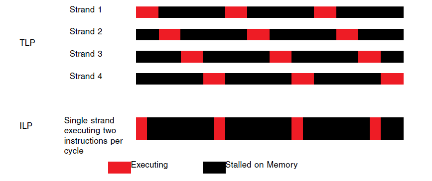
Chip Level Multithreading: It provides a control architecture for highly threaded processor implementations.

Register Window: The SPARC “register window” architecture allows for straightforward, high-performance compilers and a reduction in memory load/store instructions. Some of the windows overlap thereby reducing context switching.

Binary Compatibility: It should be compatible across different architecture for application software down to the binary level.

PROCESSOR ARCHITECTURE


UltraSPARC architecture processor contains two units:
1. IU (Integer Unit)
2. FPU(Floating Point Unit)

Virtual processor or a strand is the hardware containing the state for execution of a thread.

Physical Core is the hardware required to execute instructions.

1. IU
a) IU contains the general purpose registers and controls the overall operation of the virtual processor.
b) It performs integer arithmetic and calculates memory addressing for load/store operations.
c) Maintains program counters and controls instruction execution for FPU.


2. FPU


a) An OpenSPARC FPU has thirty-two 32-bit (single-precision) floating-point registers, thirty-two 64-bit (double-precision) floating-point registers, and sixteen 128-bit (quad-precision) floating-point registers, some of which overlap.

b) If FPU is disabled and if a call for FPU is made then either of the two things might happen:

(i) Enable the FPU and reexecute the trapping instruction
(ii) Emulate the trapping instruction in software


INSTRUCTIONS


Instructions fall into the following basic categories:


  • Memory Access
Load, store, load-store and PREFETCH instructions are the only instructions that access memory.They use two R registers or an R register and a 13 bit signed immediate value to calculate a 64 bit, byte-aligned memory address. The integer unit appends an ASI to this address.

Integer load and store instructions support byte, halfword (16 bit), word (32 bit) and extended-word (64bit) accesses


1. Memory Alignment Restrictions

A memory access on an OpenSPARC virtual processor must typically be aligned on an address boundary greater than or equal to the size of the datum being accessed, else an exception or a trap may be generated.


2. Addressing Convention

An unmodified OpenSPARC processor uses big-endian byte-order by default


3. Addressing Range


An OpenSPARC implementation supports 64 bit virtual address space. The supported range of virtual addresses is limited to two equal sized ranges at the extreme upper and lower ends of 64 bit addresses; i.e. for n bit virtual addresses, the valid address ranges are from 0 to 2^(n-1)- 1 and (2^64) - (2^(n-1)) to (2^64)-1


4. Load/Store Alternate

Versions of load-store instructions can specify an arbitrary 8-bit ASI for the load-store data access.


5. Separate Instruction and Data Memories

The interpretation of addresses in an unmodified OpenSPARC process is split; instruction references use on caching and translation mechanism and data references use another. The same underlying main memory is used.

In such split memory system, the coherency mechanism may be split so that a write into data memory is not immediately reflected in the instruction memory. Therefore self-modifying code must use FLUSH instructions to bring the instruction and data caches in a consistent state.


6. I/O Registers

The UltraSPARC architecture assumes that I/O registers are accessed through load/store alternate instructions, normal load/store instruction or read/write Ancillary State register instructions (RDasr, WRasr)


7. Memory Synchronization

Two instructions are required for synchronization of memory operations: FLUSH and MEMBAR (Memory Barrier).


  • Integer Arithmetic/Logical/Shift Instructions

These instructions compute a result that is a function of two source operands; the result is either written into a destination register or is discarded.

Shift instruction shifts the contents of an R register by a given number of bits, which is specified by the constant in the instruction or by the contents in the R register.


  • Control Transfer

Control Transfer Instructions (CTIs) include PC-relative branches and calls, register-indirect jumps and conditional traps. Most of the control transfer instructions are delayed i.e. the instruction immediately following a CTI in logical sequence, is dispatched before the control transfer to the target address is completed.

The instruction following a delayed CTI is called a delay instruction. Setting the annul bit in a conditional delayed CTI causes the delay instruction to be annulled if and only if the branch is not taken. Setting the annul bit in an Unconditional delayed CTI causes the delay instruction to be always annulled.


  • State Register Access

1. The "read" and "write" ancillary state registers read and write the contents of ancillary state registers visible to non-privileged software.

2. These registers are visible to privileged and hyperprivileged software

3. These are visible to only hyper-privileged software

  • Floating Point Operate
FPop instruction carry out all the floating point instructions


  • Condition Move
Conditional move instructions conditionally copy a value from the source register to the destination register depending on the contents of the integer register


  • Register Window Management
Register window instructions manage the register windows. SAVE and RESTORE are the non-privileged software and cause the register window to be pushed or popped. FLUSHW is a non-privileged software and causes all register windows except the current one to get flushed from the memory.

  • SIMD
Single Instruction Multiple Date are known as vector instructions.


TRAPS

A trap is a vectored transfer of control to a privileged or a hyperprivileged software through a trap table which contains the first 8 instructions of each trap handler. The base address of the trap table is contained in the state register. Part of the trap table is reserved for hardware traps and a part for the software traps.

A trap can be caused by an asynchronous request, an exception or a interrupt not directly related to the instruction.


Source: OpenSPARC_Internals_Book OpenSPARCT2_Core_Micro_Arch

Saturday, May 29, 2010

OpenSPARC Internals - Need for CMT Processors

Chip Multithreaded (CMT) Processors

Historically, microprocessors have been designed to target desktop workloads, and as a result have focused on running a single thread as quickly as possible. Single thread performance is achieved in these processors by a combination of extremely deep pipelines and by executing multiple instructions in parallel (ILP)

The processor will be idle most of the time waiting on memory, and even when it is executing it will often be able to only utilize a small fraction of its wide execution width.

It is more efficient to have a number of small, single-issue processors (meaning it can only issue one instruction in a clock cycle) that employ multi threading built in the same chip area.

Combining multiple processors on a single chip with multiple strands per processor, allows very high performance for highly threaded commercial applications. This approach is called thread-level parallelism (TLP)


With processors capable of multiple GHz clocking, the performance bottleneck has shifted to the memory and I/O subsystems, and TLP has an obvious advantage over ILP for tolerating the large I/O and memory latency prevalent in commercial applications.

Source: OpenSPARC_Internals_Book OpenSPARCT2_Core_Micro_Arch


Tuesday, May 18, 2010

Synthesis of S1 core (Simply RISC)

We decided to get working on synthesizing S1 core of Simply RISC. These were the steps I followed:

1. Install icarus-verilog from synaptic manager.
2. Extract http://www.srisc.com/download/s1_core.tar.gz
3. Read the specs http://www.srisc.com/download/simplyrisc-s1-0.1.pdf

Went to the folder in which s1 core was extracted.
In sourceme file made the following updation: export S1_ROOT=/home/aditya/SimplyRISC/s1_core

In terminal gave the following commands:

gedit sourceme
source sourceme
update_filelist
build_icarus
run_icarus
gtkwave /home/aditya/SimplyRISC/s1_core/run/sim/icarus/trace.vcd

and then from "File|Read Save File" choose the file named
"tools/src/gtkwave.sav".


Now it was time to synthesize it. I went through the same steps. After run_icarus I typed in fpga_build. But it gave the following error:


ERROR: Unable to read config file: /usr/lib/ivl/xnf.conf

: error: target_design entry point is missing.

error: Code generator failure: -2: error: target_design entry point is missing.error: Code generator failure: -2">


This was the same error at which Rudraksh was stuck. I thought this could be due to using icarus v 0.9.2 instead of 0.8 which the developers had used and I decided to install it from tarball. I also had to install flex and bison along the way. The error that I face has been logged in a text file here http://www.deorha.com/home/mtp/simply-risc . It is in errorlog_1


I decided to regress from gcc 4.4 to 4.1 due to an issue mentioned here:

http://osdir.com/ml/linux.debian.devel.ham/2007-12/msg00091.html

It didn't help.


Mr Ashish then suggested to modify build_fpga as:


iverilog -g1 -ss1_top -tnull -o fpga.edif -c$FILELIST_FPGA 2>&1 | tee synth.log


Synthesis worked after this but the synth.log was empty.

At this point it would be useful to check out http://iverilog.wikia.com/wiki/Iverilog_Flags


I replaced -tnull with -tfpga.

This time it asked for fpga.conf file instead of xnf.conf file. I downloaded icarus v0.9.2 and found fpga.conf file in it, but not present when icarus is installed from synaptic. I installed checkinstall, uninstalled icarus from synaptic and then installed icarus from source using checkinstall.


The same error repeated. Using sudo privileges I copied fpga.conf file from the source directory to /usr/local/lib/ivl. On copying strangely, fpga.conf file changed its form and it didn't open using gedit unlike earlier from the source directory. Its contents were:


functor:synth2
functor:synth
functor:syn-rules
functor:cprop
functor:nodangle
-t:dll
flag:DLL=fpga.tgt


I created a new file in /usr/lib/ivl and copied these contents in it and named it fpga.conf. Now when I ran the simulation it went one step further. But here is where I am stuck at today:


aditya@lira:~/SimplyRISC/s1_core$ build_fpga

/home/aditya/SimplyRISC/s1_core/hdl/rtl/s1_top/int_ctrl.v:47: sorry: Forgot to implement NetCondit::synth_sync

/home/aditya/SimplyRISC/s1_core/hdl/rtl/s1_top/int_ctrl.v:46: error: Unable to synthesize synchronous process.

/home/aditya/SimplyRISC/s1_core/hdl/rtl/s1_top/rst_ctrl.v:96: sorry: Forgot to implement NetCondit::synth_sync

/home/aditya/SimplyRISC/s1_core/hdl/rtl/s1_top/rst_ctrl.v:94: error: Unable to synthesize synchronous process.

/home/aditya/SimplyRISC/s1_core/hdl/rtl/s1_top/rst_ctrl.v:79: sorry: Forgot to implement NetCondit::synth_sync

/home/aditya/SimplyRISC/s1_core/hdl/rtl/s1_top/rst_ctrl.v:77: error: Unable to synthesize synchronous process.

/home/aditya/SimplyRISC/s1_core/hdl/rtl/s1_top/spc2wbm.v:162: sorry: Forgot to implement NetCondit::synth_sync

/home/aditya/SimplyRISC/s1_core/hdl/rtl/s1_top/spc2wbm.v:159: error: Unable to synthesize synchronous process.

:0: sorry: Forgot to implement NetBlock::synth_sync

/home/aditya/SimplyRISC/s1_core/hdl/rtl/sparc_core/cluster_header.v:335: error: Unable to synthesize synchronous process.

ivl: synth2.cc:212: virtual bool NetCase::synth_async(Design*, NetScope*, const NetBus&, NetBus&): Assertion `statement_default == 0' failed.

Aborted


The log file is attached on this page http://www.deorha.com/home/mtp/simply-risc. It is errorlog_2


This was also written in the synth.log file. I have also been given an idea by Ashutosh that I should try synthesizing it in centOS in a Virtual Box. That's what my agenda for today is.

Simply RISC

As was mentioned in the earlier post, there were problems with synthesizing SPC of OpenSPARC. Also the following observations were made:

1. http://wienker.org/blog/?p=144 It is mentioned that it took 4.5 GB almost to synthesize a single core. With the current hardware available (3.3GB memory in the computer allotted to us), we cannot synthesize it.

2. http://fpga.sunsource.net/ It can be seen that the no. of LUTs required by SPC alone is about 60,000 which is pretty huge.

3. Instead of synthesizing SPC from SPARC's code, we can try working on SimplyRISC S1 core which is a cut down version of OpenSPARC T1, having just one core and importantly with ccx replaced by a wishbone.

http://en.wikipedia.org/wiki/S1_Core

http://www.srisc.com/?home

The cool thing about working with this is that it has been synthesized on Icarus Verilog Synthesizer. http://www.icarus.com/eda/verilog/ and the complete procedure is given on the developer's website.

http://news.techworld.com/operating-systems/6849/say-hello-to-open-source-hardware/

2. http://fpga.sunsource.net/ It can be seen that the no. of LUTs required by SPC alone is about 60,000 which is pretty huge.3. Instead of synthesizing SPC from SPARC's code, we can try working on SimplyRISC S1 core which is a cut down version of OpenSPARC T1, having just one core and importantly with ccx replaced by a wishbone. http://en.wikipedia.org/wiki/S1_Corehttp://www.srisc.com/?homeThe cool thing about working with this is that it has been synthesized on Icarus Verilog Synthesizer. http://www.icarus.com/eda/verilog/ and the complete procedure is given on the developer's website. http://news.techworld.com/operating-systems/6849/say-hello-to-open-source-hardware/">

We decided to work on synthesizing S1 core of Simply RISC. And after that we wished to extract FPU from T1/T2 and synthesize it alone.

First Attempt at OpenSPARC SPC synthesis

My first attempt at OpenSPARC Single Processor Core (SPC) synthesis didn't succeed. Actually even the 2nd, 3rd and 4th attempt didn't succeed.

My first attempt was made on a 1GB computer in Digital Hardware Design (DHD) lab in Bharti Building. It gave an error issue with the memory. I switched over to a 3.3GB PC.

On that PC too, it gave some internal error. Now the problem I believe was this. We wanted to synthesize Single Processor Core and not T2 which would've included all the 8 cores. spc.v was a below t2.v source file when all the source files were added. But when I set spc.v as top module, I wasn't getting an option to synthesis in Xilinx ISE. But when I use to specify t2.v as the top module, only then did I get an option to synthesize. So my intuition says that it was trying to synthesize all the 8 cores. Why? Let us take a look at the script used to synthesize spc and t2.

$DV_ROOT/tools/fpga/fpga_synth -synplicity -top spc

$DV_ROOT/tools/fpga/fpga_synth -synplicity -top t2

i.e. only the top module is different for spc and for t2.

The file list needed to be added for both spc and t2 was located at:
$DV_ROOT/tools/fpga/fpga_synth

Therefore we reached a roadblock which we were unable to clear.

At the same time Mr. Ashish was trying to locate an open source toolkit chain. He came across one prospective Icarus Verilog, an open source verilog code synthesizer and simulator.

Ideas by Mr. Ashish

Getting Started with OpenSPARC
Step 1:
Read Mr. Ashish's Blog on OpenSPARC Internals ...http://fpga.ashishbanerjee.com/opensparc This should give you an overview of OpenSPARC design.

Step 2:
Synthesize an OpenSPARC core into an FPGA.
The steps are detailed in OpenSPARC Internals book, Chapter 6.
See the OpenSPARC T1 FPGA Video here: http://www.youtube.com/watch?v=ZCX03bU8TSM

Project Ideas

Short Term Projects (BTech Level):
  • Extract NIU (Network Interface Unit) and synthesize it on a FPGA
  • Extract the Cryptographic Accelerator and synthesize it on a FPGA
  • Create a DDR3 interface for OpenSPARC (Presently supports DDR2).
  • Identify a Java server side application and tune it to make it run faster on CMT (Chip Multi-Threading) Architecture. See my paper here:
  • Compare Power7 Architecture with OpenSPARC T1 Architecture.
  • Optimize a MegaCell for FPGA (6-LUT , 4-LUT and 3-LUT architectures).

Long Term Projects (MTech/PhD Level):
http://fpga.ashishbanerjee.com/ideaz
 
/* Google Analytics ----------------------------------------------- */